
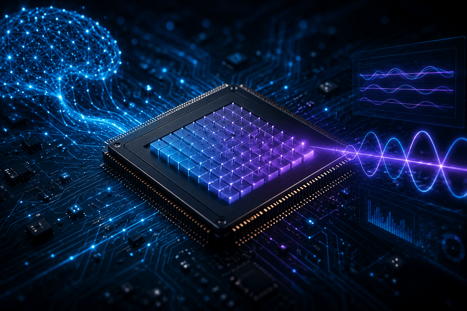
The dominant approach to AI computing — train a model on thousands of GPUs, store weights in DRAM, and move data back and forth billions of times per second — works. But it is also extraordinarily energy-intensive and generates immense heat. TetraMem, a Silicon Valley semiconductor startup, is betting there is a fundamentally better way. The company has announced the successful tape-out, manufacturing, and initial silicon validation of its MLX200 platform — a 22nm multi-level RRAM-based analog in-memory computing system-on-chip produced on a commercial TSMC process. The milestone represents seven years of research translated into manufacturable silicon, and a meaningful step toward commercialising an AI computing architecture that moves computation into memory rather than moving data to the processor.
The Memory Bottleneck: Why AI's Data Movement Problem Is Getting Worse
As AI workloads scale, a structural constraint is becoming increasingly apparent: the von Neumann bottleneck. In conventional computing architectures, processors and memory are physically separate. Every operation requires data to travel between them — consuming energy, introducing latency, and generating heat proportional to the volume of data moved. For large AI models running inference at scale, this movement of data is not incidental overhead; it is often the dominant source of energy consumption and the most significant latency constraint.
Edge AI applications face this challenge in its most acute form. Devices like wearables, IoT sensors, hearing aids, and always-on voice interfaces must run AI workloads continuously and locally — without the luxury of a data centre's power budget or cooling infrastructure. The energy cost of moving data between memory and compute is often the single factor that makes always-on AI impractical in constrained environments. Reducing or eliminating that movement is the fundamental design objective of in-memory computing.
What RRAM and Analog In-Memory Computing Actually Do
Resistive RAM (RRAM) — also called memristor technology — is a type of non-volatile memory that stores information as the electrical resistance of a material junction. Unlike conventional DRAM, which stores data as a charge state (on or off), RRAM cells can be programmed to a large number of intermediate resistance levels, enabling multi-level storage — effectively encoding multiple bits of information per cell. TetraMem's technology has demonstrated up to 2,048 conductance levels per cell — equivalent to 11 bits of precision — in fully integrated 256×256 arrays on CMOS, as published in Nature in 2023.
Analog in-memory computing (IMC) goes further: rather than simply storing data in RRAM cells and then reading it out for computation elsewhere, it performs vector-matrix multiplications — the core mathematical operation of neural network inference — directly inside the memory array. The electrical properties of the RRAM cells perform the computation in parallel as current flows through the crossbar array, using Ohm's Law and Kirchhoff's Current Law as the fundamental physics of computation. The result is that data never needs to leave memory to be processed, dramatically reducing the energy and latency costs of AI inference.
"This milestone reflects years of close collaboration with our foundry partner TSMC and demonstrates the feasibility of bringing multi-level RRAM and analog in-memory computing from computing architecture breakthrough into advanced-node commercial silicon."— Dr. Glenn Ge, Co-founder & CEO, TetraMem
The MLX200 Platform: What Was Achieved and What It Means
The successful tape-out, manufacturing, and initial silicon validation of the MLX200 at TSMC's commercial 22nm process node is the critical gate between research demonstrator and manufacturable product. Achieving tape-out at a commercial foundry on an advanced process means the design has passed the rigorous engineering, design rule, and manufacturing checks required for real-world production — not just for a one-off lab chip but at a process that can, in principle, scale to volume.
The MLX200 integrates multi-level RRAM arrays with mixed-signal compute engines, enabling high-throughput vector-matrix operations to be performed directly within memory. Key technical attributes of the 22nm RRAM implementation include CMOS compatibility with minimal additional process complexity, low-voltage and low-current operation, strong retention and endurance characteristics, and the multi-level capability required for high compute density. Early silicon results have demonstrated consistent functionality across arrays — the critical validation signal that the approach is viable for both embedded non-volatile memory and compute-in-memory applications at this node.
The MLX200 and its companion MLX201 are targeted at power- and latency-sensitive edge AI applications: voice and audio processing, wearable devices, IoT systems, and always-on sensing. Evaluation kit (EVK) sampling is targeted for the second half of 2026, and TetraMem's multi-level RRAM memory IP is available for evaluation and potential licensing by system partners.
Why This Milestone Matters for the Future of AI Computing
The significance of the MLX200 milestone is not primarily in what the chip can do today — it is in what it proves is possible tomorrow. Getting multi-level RRAM and analog in-memory computing through a commercial tape-out at TSMC 22nm with consistent silicon results is a proof-of-manufacturability that the broader semiconductor and AI infrastructure industries have been watching for. Research demonstrators on custom processes have existed for years; commercial viability on a mainstream TSMC node with real device uniformity across large arrays is a qualitatively different achievement.
The global AI infrastructure buildout is currently consuming enormous and growing quantities of energy. Data centre power demand is on a trajectory that intersects with grid capacity constraints in multiple major markets. Any approach that can deliver competitive AI inference at materially lower energy consumption — without sacrificing speed or accuracy — represents a significant commercial opportunity and a potential contribution to the sustainability of AI at scale. TetraMem's vision, from edge wearables to 3nm cloud-scale GenAI, is that analog in-memory computing built on RRAM can be that approach — and the MLX200 is the first commercial silicon evidence that it may be right.